


-1-360x180.jpg)


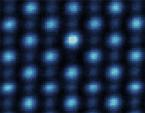
It’s been 37 years since scientists first demonstrated the ability to move single atoms, suggesting the possibility of designing materials atom by atom to customize their properties. Today there are several techniques that allow researchers to move individual atoms in order to give materials exotic quantum properties and improve our understanding of quantum behavior.But existing techniques can only move atoms across the surface of materials in two dimensions. Most also require painstakingly slow processes and high-vacuum, ultracold lab conditions.Now a team of researchers at MIT, the Department of Energy’s Oak Ridge National Laboratory, and other institutions has created a way to precisely move tens of thousands of individual atoms within a material in minutes at room temperature. The approach uses a set of algorithms to carefully position an electron beam at specific locations of a material, then scan the beam to drive atomic motions.“The results demonstrate the ability to deterministically move atoms repeatedly within a material’s 3D atomic lattice,” says MIT Research Scientist Julian Klein, who conceived of and directed the project. “We can reprogram materials to create defects at will, realizing entirely artificial states of matter not found in nature with a wide range of potential applications, including sensing, optical, and magnetic technologies. There are so many opportunities enabled by these techniques.”“It’s like a photocopier that can create columns of identical atomic defects,” says Frances Ross, MIT’s TDK Professor in Materials Science and Engineering. “It’s especially useful because you can move a few atoms to form defects, and do it again and again to build atomic arrangements in three dimensions that have tunable functions in a system that is more robust because the defects exist beneath the surface.”In a Nature paper appearing today, the researchers described their approach and how they used it to create more than 40,000 quantum defects in a crystalline semiconductor material.The researchers say the approach offers a new way to study quantum behavior in materials. It could also one day lead to improvements in systems that leverage quantum defects, like quantum computers, dense magnetic memory, atomic-scale logic devices, and more.Joining Klein and Ross on the paper are Kevin Roccapriore and Andrew Lupini, researchers at Oak Ridge National Laboratory; Mads Weile, a former MIT visiting student; Malte Rösner and Sergii Grytsiuk, former Radbound University researchers; Zdenek Sofer, a professor at the University of Chemistry and Technology Prague in the Czeck Republic; Dimitar Pashov, a research associate at King’s College London; and Mark van Schilfgaarde and Swagata Acharya, researchers at the National Laboratory of the Rockies.Designing matterIn a now-famous 1989 demonstration, IBM researchers used a scanning tunneling microscope to arrange 35 atoms on the surface of a chilled crystal to spell out “IBM.” It was the first time atoms had been precisely positioned, and an important milestone. The approach enabled scientists to engineer specific defects, such as atom-sized vacancies and surface atoms in crystalline materials, leading to major advances in quantum science. But placing those 35 atoms had taken researchers many hours, if not days.In parallel with those developments, researchers also developed two additional approaches for manipulating atoms in a vacuum, using optical tweezers to trap neutral atoms and oscillating electric fields to trap ions.While those approaches have enabled remarkable progress, they remain limited to either surfaces or highly controlled experimental systems. Another factor limiting the design of materials for applications such as quantum computers is the inability of atomic manipulation techniques to move atoms in three dimensions: The patterns are created on the surface of a material, where they are exposed to the environment and cannot survive outside tightly controlled laboratory settings.Engineering usable materials with custom quantum properties would require researchers to rearrange many more atoms, preferably on the interior of materials. The MIT researchers demonstrated that capability in their Nature study.“We were trying to improve the number of atoms we could move in a reasonable length of time,” Ross explains. “You want to place the atoms close to each other so they can interact, and you want to have a lot of them arranged as you’d like — thousands or millions of atoms in specific locations you’ve chosen. That’s been challenging with existing techniques.”The researchers used high-performance microscopes at the Department of Energy’s Oak Ridge National Laboratory for their work. Their new technique uses a sophisticated set of algorithms to direct an electron beam at a target atom with a precision of a few picometers (one trillionth of a meter). The beam does a tight loop to help zero in on its target, then sends a beam of electrons through the material in a carefully designed oscillating path, spending about a second at each location. “We developed algorithms that allow us to quickly obtain information on where the beam is in the material,” Klein explains. “The trick is to use very few electrons in the process of getting that information, so the whole process is fast and does not unintentionally damage your crystal. It took many years to develop these algorithms and determine the minimum required information needed to infer where the atoms are located with the highest precision.”The motion of the beam as it delivers electrons, an oscillating path devised by the researchers, pushes entire columns of atoms to new locations the way you might swipe a screen on your phone.In their experiments, the researchers used this approach to direct the movement of columns of chromium atoms in a stable semiconductor material, chromium sulfide bromide, using a crystal about 13 nanometers thick. The beam created atom-sized vacancies in the material, each vacancy paired with the displaced atom, that they calculated would give the crystal exotic quantum properties.To show how well their approach scaled, the researchers created over 40,000 defects in about 40 minutes, creating vacancies and interstitials across different distances and in different patterns, calculating that different atomic arrangements should give rise to different quantum mechanical properties.“Each of these defects has certain ways to interact with its neighbors,” Ross says. “If you place them in a pattern, you could essentially simulate the interactions between the electrons within a molecule, so the whole electronic structure of that molecule can, in a sense, be mapped onto a pattern that you can write into a solid material.”Probing quantum systemsThe success of the approach was likely aided by the way chromium binds within the semiconductor, which has a unique electronic structure. The researchers are further investigating other crystals in which this might work, though they suspect it will be applicable to a diverse range of materials. In the materials where it works, the approach has several advantages over existing techniques.“Moving atoms within solids enables the creation of quantum properties in materials that are stable in the air outside of vacuum conditions,” Klein explains. “And this approach is also scalable to many atomic manipulations, so moving thousands or millions of atoms to create artificial structures would represent completely new physics. We’d like to study those systems.”The researchers say their technique lays the foundation for a new class of programable matter, which could aid the development of a range of stable quantum devices.“This is a way of accessing physical phenomena that involve a lot of atoms placed in a certain specified arrangement, and can’t be done by self-assembly,” Ross says. “You can create individually tuned atomic arrangements, and you can have so many of them, each arranged exactly how you like over areas that are tens and hundreds of nanometers. That leads to collective physics we are excited to explore.”The work was supported, in part, by the Department of Energy and the National Science Foundation.

- Trending
- Comments
- Latest


Recent News

Stay ahead with the latest insights on Hong Kong’s economy, finance, and investments. From market trends to policy updates, we bring you in-depth analysis and expert opinions.
📩 Subscribe to our newsletter for exclusive updates.
📍 Follow us on social media for real-time news.
📧 Contact us: info@hongkong-invest.com